
Materials with Controlled Emissivity
SensorMetrix has undertaken R&D projects to develop infrared metamaterials and other exotic electromagnetic materials with controlled emissivity.
In metamaterials, independent manipulation of permeability (ε) and permittivity (μ) results in the ability to tailor the index of refraction to approximately match the impedance Z(w) to free space, i.e. ε ~ μ → Z=Z0 and minimize the reflectance at a specific frequency.
R = 1-T-A
where R is reflectivity, T is transmission and A is absorption.
When the material is impedance-matched, the transmission is governed by the quantity n2kd, (k is the wavevector and d is the absorber thickness), which can be simultaneously tuned with Z to obtain high absorption. It is possible to design metamaterials with impedances systematically varying from the free space value (Z0), to values as low as Z(w)→0 or as high as Z(w)→∞. By simultaneously tuning n2 to minimize transmission (T→0) the whole absorptivity/emissivity range from black body (A→1) to reflective metallic surface (A→0) can be achieved.
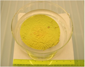
Features:Near Black Body absorber – SensorMetrix personnel was on the team that demonstrated the first metamaterial IR perfect absorber (absorption ~ 1 was demonstrated in MWIR)
Very thin films (smaller than wavelength) – as compared to conventional absorbers, a very high absorption can be achieved in a very thin film. A typical metamaterial IR absorber has a thickness less than 0.5 um consisting of a dielectric layer and patterned metamaterial metallization Large area fabrication – we have fabricated infrared absorbers using conventional wafer level processing as well as roll-to-roll processing techniques. |
Free standing metamaterial absorber film
|
Narrow or wide band – depending upon constitutive materials and specific designs ultra-narrow or extremely wide band absorbers can be implemented.
On-demand spectral control – we have demonstrated that metamaterials can be fabricated with absorption (emission) peaks at arbitrary frequency from short wave infrared (SWIR) to millimeter waves. Single and dual-band absorbers were demonstrated.
On-demand spatial absorber – areas of high and low emissivity can be laterally distributed in arbitrary fashion. Absorber areas as small as 7x7 μm were demonstrated. Wafer size absorbers can be fabricated and tiled to enable larger areas.
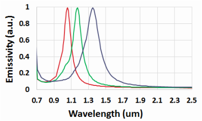
Narrower and wider band emitters
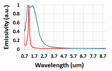
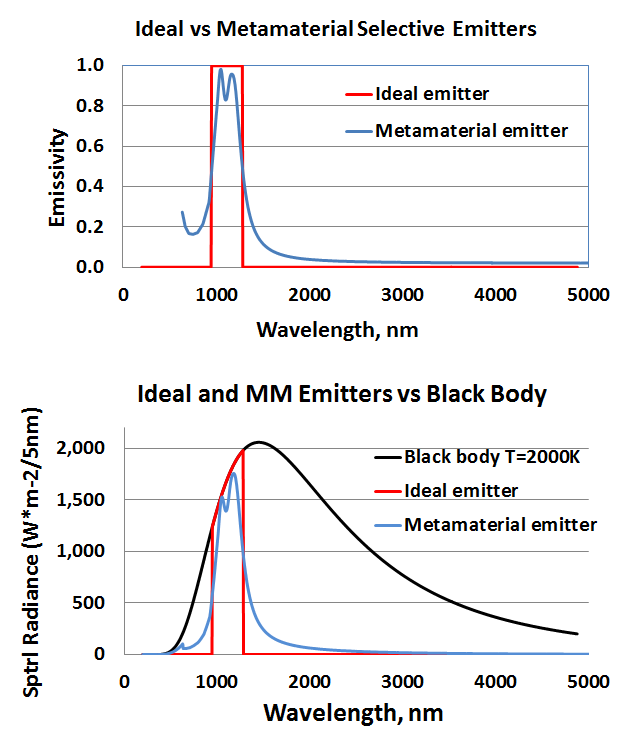
Selective emitter - Metamaterial selective emitters can be engineered to have high emissivity (ε ~ 1) in a specified frequency range and very low emissivity outside of this range. The SensorMetrix team has demonstrated a range of selective emitters, with on-demand spectral profiles from SW- to LWIR with the bandwidth that can be readily tailored for spectral position, bandwidth, as well as sharp band edges. ApplicationsSensorMetrix has been developing IR electromagnetic materials and metamaterials for a wide range of applications including:
- Controlled emissivity - TPV efficient power conversion - Solar power conversion - Directive emission – thermal management for aero-space applications - IR emitter for display applications - IR Detectors & sensors |
Spectral control of emissivity
|